Ultra-fine-pitch Assembly and Test
3D ICs can enable memory on memory, memory over logic, logic over logic using interconnect technologies such as TSV, redistribution layers (RDL) containing interconnect wiring and micro-vias, copper pillar micro-bumps/solder bumps, and flip chip bonding or the emerging copper hybrid bonding first proven by Sony for complementary metal-oxide semiconductor (CMOS) image sensors for inter-die communication.
3D ICs allows for vertical stacking of heterogeneous dies from different manufacturing processes and nodes, chip reuse and chiplets-in-SiP (system-in-a-package) for high-performance applications already pushing the limits of a single die at the most advanced node. Monolithic 3D ICs build on multiple active silicon layers with vertical interconnects between layers.
To accelerate adoption, 3D IC systems must be architected in a more holistic way via IC-package-system co-design which involves the silicon IP, ICs/chiplets and IC package and addresses accompanying power and thermal challenges.
Challenge
Although 3D ICs enable significant benefits compared to 2D integration, there exist a noticeable divide or asymmetry between the dimensions of transistors and the dimensions of TSVs in active dies.
Today, the channel length of modern transistors has already reached 10 nm or less, which is far smaller than the diameter of typical TSV diameters of a few micrometers in active ICs.
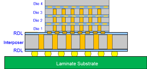
In addition, there exist divides in the L/S, the pitch of through vias and interconnect bonding pad pitch:
- between wafer BEOL and interposer processes
- between interposer processes and IC substrate processes
- between IC substrate processes and PCB processes at the system level.
Regardless of the advanced SiP styles, the mainstream, best-can-do line width (L)/ spacing (S) deployed in advanced SiPs today is typically around 0.2 μm/0.2 μm, 2 μm/2 μm, and 6 μm/6 μm, respectively, for wafer BEOL, 2.5D/3D/fan-out and ABF based laminate substrate with corresponding interconnect layer thickness at ~ 1 μm, ~5 μm, and 20 μm.
In contrast, the plated through holes in build-up laminate substrates can be as small as 30 μm in diameter at a pitch of around 50 μm. Corresponding through hole dimensions for PCB often times are far larger than those for IC substrates and tend to vary widely by application.
Mainstream ultrafine-pitch micro-bump solder based flip chip can achieve a bond pitch of ~40 μm for chip to chip bonding, whereas the solder-less copper hybrid bonding technique for chip to chip bonding or bonding of silicon layers is capable of a bond pitch of 6-10 μm today and beyond.
The above chip/package/system interconnection divides or asymmetries presents a significant limitation on the density and granularity that can be achieved by 3D IC integration.
Bridging the Chip/Package/System Divides to Enable Novel 3D IC Packaging
- Resolve the problem for denser 3D IC stacking
- Resolve the problem for denser 3D IC to interposer interconnection
- Resolve the problem for denser laminate to PCB interconnection
- Overcome the ultra-fine-pitch testing