Contact
 MENU
MENU

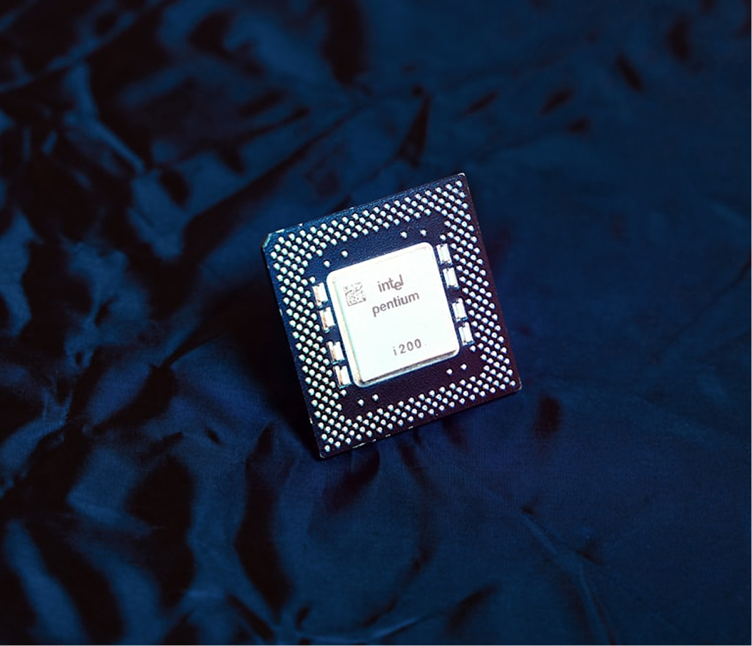
The advent of 5G/6G, AI, xEV, IoTand metaversehas spurred a plethora of new end use applications, leading to an exponential growth in data communication in 3C, namely, data centers, base stations and commercial/edge electronics.
To process the escalating data traffic, high performance computing and data centers (HPC) involving advanced system-on-chips (SoCs) and advanced system-in-a-packages (SiPs) will incessantly demand highest processing rates, highest communication rates (lowest latencies, highest bandwidth, and often both of these) and highest storage capacities with “extreme requirements” for IC and IC packaging that address the ever-more stringent interconnection requirements and ever-higher power dissipations.

from ever-bigger processor SoCdie to disaggregated small die based chiplets-in-SiP

challenge icon
Evolution of Computing Architectures
from traditional computing to near-memory computing (2.5D IC) to in-memory computing (via 3D IC or 3D monolithic IC) to reduce the memory or bandwidth wall between processor and memory at the system level in order to more fully exploit the processor performance potentials

from copper interconnect to optical interconnect

from advanced organic laminate substrate to silicon interposer and hybrid substrates with embedded active devices.

Lorem Ipsum is simply dummy text of the printing and typesetting industry. Lorem Ipsum has been the industry's standard dummy text ever since the 1500s, when an unknown printer took a galley of type and scrambled it to make a type specimen book.

Lorem Ipsum is simply dummy text of the printing and typesetting industry. Lorem Ipsum has been the industry's standard dummy text ever since the 1500s, when an unknown printer took a galley of type and scrambled it to make a type specimen book.
